Describing and Checking a Chiplet Stack, With Open Tools
A 2.5D/3D assembly is a description of how several dies are placed, flipped and bonded — not a design file. Here is how you write one, what can be checked about it, and how to get a drawing out, with open tools and no GUI.
August 2, 2026 • By Shivaram Mysore
This is the first post in a three-part series on open chiplet tooling. It introduces the assembly model: how a chiplet stack is described, validated and visualized. The second explains why structural verification alone is insufficient, and the third shows how the pieces come together into an open chiplet workflow.
Every chiplet flow has to answer three questions:
- How is the assembly described? — the representation layer
- Is the assembly correct? — the verification layer
- Can it be built? — the implementation layer
This series covers the first two, which now work with open tools. The third is where this is going — and the honest state of it is step one.
This post answers the first question.
An assembly is a different kind of file
A design file — Verilog, DEF, GDS — describes one chip. An assembly describes how several chips relate to each other: which die sits where, which way up each one is, and which surfaces are bonded together.
That last part is the unfamiliar one. A die has a front (transistors and wiring) and a back (bare silicon). For a normal chip this never comes up. For a chiplet it decides everything: two dies can only be joined where their surfaces meet, and which surface faces which way depends on whether the die was flipped over during assembly.
The interchange format for this is 3Dblox. It comes in two files:
- a
.3dbvdefines the chiplets — each die's size, thickness, and its bonding surfaces - a
.3dbxdefines the assembly — where each die instance sits, how it is oriented, and which surfaces connect
Here is a complete two-die stack. The definitions first:
ChipletDef:
  compute:
    type: die
    design_area: [2000, 2000]     # microns
    thickness: 250
    regions:
      front:                       # a bonding surface on the front face
        side: front
        coords: [[0,0], [2000,0], [2000,2000], [0,2000]]
        bmap: compute_front.bmap   # the bump map for this surface
  memory:
    type: die
    design_area: [2000, 2000]
    thickness: 180
    regions:
      front:
        side: front
        coords: [[0,0], [2000,0], [2000,2000], [0,2000]]
        bmap: memory_front.bmap
Then the assembly:
Stack:
  u_compute: {loc: [0.0, 0.0], z: 0.0,   orient: R0}
  u_memory:  {loc: [0.0, 0.0], z: 250.0, orient: MZ_MY}

Connection:
  d2d:
    top: u_memory.regions.front
    bot: u_compute.regions.front
Read that last block in English: the memory die's front surface bonds to the compute die's front surface. Face to face. The memory die sits at z = 250 µm, which is exactly the thickness of the compute die beneath it, and it is flipped (MZ_MY) so that its front points down into the joint.
Where the paths point
One detail that costs people an afternoon: every relative path in these files resolves against the file that names it, not against your working directory. The .3dbx includes a .3dbv relative to itself; the .3dbv names its bump maps relative to itself. So the whole assembly can live in a directory and be checked from anywhere:
vyges opendb check-d2d --input designs/stack.3dbx # works from any cwd
APR_tech_file entries may also contain * globs and are expanded where the pattern points, and a #!define macro at the top of a .3dbv is substituted before any of that happens.
Reading it in
vyges opendb read-3dblox --input stack.3dbx --output stack.odb
That builds the chips, bonding regions, die-to-die connections and bumps in a design database, and writes it out. The database here is OpenDB, the design database at the heart of OpenROAD, and the reason any of this is possible in the open. The division of labour is simple: OpenDB provides the data model; Vyges™ Loom provides the executable workflows built on that model — reading assemblies, validating them, checking die-to-die interfaces and producing visualizations. The 3D data model is OpenDB's: the chip and bonding-region classes, the die-to-die connections, and the unfolded model, which resolves a nested stack into absolute positions so you can ask where a given bump actually ends up in the finished assembly.
What the reader cannot represent, it names rather than dropping:
read-3dblox: 1 element(s) the database cannot represent:
  connection soc_to_virtual (virtual, no bottom)
That matters more than it looks. A bump map that silently failed to load would leave every bump-related check with nothing to look at — and a clean verdict to show for it. "We looked and found nothing" and "we did not look" have to be different answers.
Checking it
vyges opendb check-3dblox --input stack.odb
Seven structural checks run over the assembly: logical connectivity, floating chips, overlapping dies, unused internal surfaces, bond-region overlap and mating-surface gap, bump alignment, and alignment markers. The report names the findings, not just a count:
{ "violations": 2,
  "categories": [
    { "category": "Floating chips", "count": 1,
      "markers": [{ "comment": "Isolated chip set starting with u_compute" }] },
    { "category": "Connection regions", "count": 1,
      "markers": [{ "comment": "Invalid connection memory_to_interposer: u_memory/front (faces TOP) to u_interposer/front (faces TOP)" }] }]}
That second finding is a real mistake we made while building the interposer example for this series, and it is a good illustration of what the structural checks are for. We had two dies sitting on an interposer, each bonding its front to the interposer's front — and got told, correctly, that both surfaces face upward and therefore cannot mate. A die mounted on an interposer has to be flipped so its front faces down. The checker caught the modelling error before the drawing did.
It is a checker, not a repairer: it annotates the in-memory database and never modifies the design.
The measurement that stopped us shipping something wrong
Here is the part worth taking away even if you never touch a chiplet.
To draw a flipped die correctly — and to check its bumps — you need to know what each orientation does to coordinates. The names look self-explanatory. MZ is "mirror in Z", so surely it flips the die over and mirrors it.
We measured it instead, by placing a bump at a known point under every orientation and reading back where the database said it ended up:
| orientation | where a bump at (2.84, 3.36) lands |
|---|---|
R0 |
(2.84, 3.36) |
MY |
(47.16, 3.36) — mirrored in X |
MX |
(2.84, 36.64) — mirrored in Y |
MZ |
(2.84, 3.36) — unchanged |
MZ_MY |
(47.16, 3.36) — flipped and mirrored |
MZ does not mirror anything in X or Y. It flips which face points up and leaves the bump field's handedness alone. The mirror people expect from the word "flipped" comes from the MY component — so a face-to-face die is usually MZ_MY, not MZ.
Had we reasoned from the names, we would have drawn a plausible, confident, wrong picture of every flipped die, and checked interfaces in a mirrored frame. It would have looked fine. That is the failure mode worth fearing: not the tool that crashes, but the one that answers smoothly and incorrectly.
The lesson wasn't "read the documentation." It was "measure the implementation."
The same instinct shows up in what the tool refuses to do. An orientation string we have not verified is rejected outright rather than processed, because the database silently treats anything it does not recognise as R0 — inheriting that would place a die wrongly and then report the interface clean.
Drawing it
The thing we did not expect to build. A 2D layout viewer is genuinely hard — a routed block is millions of polygons, so viewing one needs a tile server, a spatial index and a raster pyramid. A chiplet assembly is almost embarrassingly simple by comparison. A stack is a handful of dies, each a box, with a few bonding regions: tens of rectangles, not millions.
So the viewer that is out of reach at layout scale is a few hundred lines here, with no server, no GUI toolkit and no X:
vyges opendb view-3dblox --input stack.3dbx --output stack.svg
vyges opendb view-3dblox --input stack.3dbx --output stack.png --scale 2
The output extension picks the format. SVG is exact and diffable, so it belongs in a repository or a CI artifact; PNG is what goes into a slide or a message. Both come from one layout, so they cannot drift into being pictures of different things.
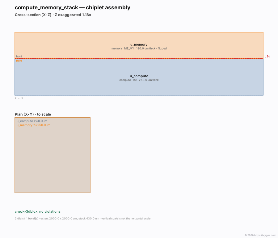
Two views, because one is not enough. The plan view at the bottom — the assembly seen from above — shows footprints and overhang. It cannot show stacking order, die thickness, bond gaps, or which face is bonded, and those are the entire subject. So the primary view is the cross-section at the top: a slice through the package, as if you sawed it in half and looked at the cut edge. That is where you can see the compute die at the bottom, the memory die above it, the red dashed bond line between them, and the word front on both sides of that line — the face-to-face joint.
The vertical axis is stretched, and the drawing says so in its own caption. A die is millimetres across and microns thick; drawn to one scale the stack would be a line.
How this sits on OpenDB
vyges-opendb is a Rust API over OpenDB with no Tcl, no SWIG, and no OpenROAD engines. It pins an OpenROAD commit, does a sparse checkout of just the database sources, and compiles a standalone static library — so the result is a single binary with no runtime library to find and nothing to configure. No Python, no interpreter, no virtualenv: on Linux it is an 8 MB executable that links the C runtime and zlib and nothing else. Download a file, run it.
That boundary is deliberate, and we learned it the expensive way on a previous engine: linking a large tool to borrow one reader dragged in a Tcl interpreter, a pinned submodule and a segfault. The rule we now follow is to integrate at the file format, not the library, and to bind the database directly rather than the tools built on it.
Everything above runs from one binary:
vyges install loom # includes vyges-opendb
What is not there yet
Worth stating plainly, because "chiplet support" is being used loosely at the moment.
You can describe an assembly, check its structure, check its die-to-die interfaces, and draw it. You cannot time a 3D stack — cross-die timing and 3D parasitic extraction need database classes that do not exist upstream at the version we build against. Writing 3Dblox back out is not there either. And a stack whose dies sit on genuinely different processes cannot be fully represented, because a design database holds one technology — which is awkward, given that heterogeneity is the entire premise of chiplets. That one is upstream's constraint, not ours, and it is why we describe this as an assembly description rather than a heterogeneous stack.
Those gaps are real, and we would rather name them than let the phrase imply they are solved. What is true today is narrower and still useful. One assembly description goes in, and three independent products come out:
- a structural verdict — is the stack physically coherent?
- an interface verdict — do the die-to-die connections actually connect?
- a cross-sectional visualization — what does it look like?
Entirely with open tools, on your own machine. That is enough to make advanced packaging a practical open-source workflow, rather than just an interchange format.
vyges-opendb is part of the Vyges Loom open EDA suite — Apache-2.0, built on OpenROAD's OpenDB (BSD-3-Clause). 3Dblox is an open interchange format for 2.5D/3D assemblies.