Open-Source EDA Now Has a Chiplet Workflow
You can now describe a chiplet assembly, verify it, and see it — end to end, with open tools. Here is what that means, and what it does not.
August 11, 2026 • By Shivaram Mysore
Until now there was no complete open workflow for chiplet assembly verification. That changes today.
Open-source EDA has covered implementation for years: RTL, synthesis, place-and-route, timing, DRC, LVS. Advanced packaging was not on that path — chiplet assembly lived entirely in commercial tools, priced as a tier above ordinary implementation, which meant the people most likely to need chiplets and least able to afford that tier had no way in.
You can now describe a chiplet assembly, check that it is structurally sound, check that its die-to-die interfaces actually connect, draw it, and gate CI on all of it — with open tools, on your own machine.
Here is why that matters, and what it still does not do.
Why chiplets, briefly
If you have not had reason to care about this yet, the short version is that the industry ran into three walls at once.
Size. There is a hard limit on how large a single die can be — the reticle, the maximum area a lithography scanner can print in one exposure. The largest designs have reached it. You cannot simply make the chip bigger.
Yield. Defects scale with area, and they scale badly. Four small dies that each yield well are dramatically cheaper to produce than one large die of the same total area, because a defect kills a quarter of your silicon instead of all of it.
Fit. Not every function wants the same process. Logic benefits from the newest, most expensive node. Analog, I/O and memory frequently do not — they work better, or merely cheaper, on an older one. A single die forces one choice for everything.
Chiplets answer all three: build several smaller dies, each on the process that suits it, and join them into one package. The cost moves from the silicon into the assembly — into getting the joining right. Which is precisely the step that had no open tooling.
If your work is RTL and physical design, this is becoming your problem rather than someone else's. Past the reticle limit there is no "make the chip bigger" option, so the assembly stops being something that happens after your job ends: the die-to-die interface is part of the design, and getting it wrong invalidates two perfectly good implementation runs. Advanced packaging is turning into a natural extension of digital implementation rather than a separate niche.
OpenROAD's mission has largely been read as implementing a single die. OpenDB's 3D model quietly extended that foundation into advanced packaging. The tooling here is an attempt to make that capability directly usable.
What exists now
Four commands, one binary, no GUI and no licence server:
vyges opendb read-3dblox  --input stack.3dbx --output stack.odb   # read the assembly
vyges opendb check-3dblox --input stack.odb                       # is it structurally sound?
vyges opendb check-d2d    --input stack.3dbx                      # do the interfaces connect?
vyges opendb view-3dblox  --input stack.3dbx --output stack.svg   # what does it look like?
Each emits JSON and exits non-zero on a violation, so they gate CI directly.
It is one Rust binary — no Python, no Tcl, no interpreter, nothing to install but the file itself — and every command describes its own interface, so an AI assistant can drive it through the built-in MCP server as easily as you can from a shell.
The credit for the foundation is not ours. OpenROAD's OpenDB is where the open chiplet data model came from — dies, bonding surfaces, die-to-die connections, and a stack that resolves to real positions. The division of labour is simple:
OpenDB provides the data model. Vyges™ Loom provides the executable workflows built on that model.
The failure it was built to catch
Two dies are only connected if the microbumps on their mating faces physically land on each other and carry the same signals. Get that wrong and you have a package that assembles, powers up, and does nothing.
We took a working two-die assembly and made a one-character change to its description — a die that should have been flipped and mirrored was marked only as flipped. The entire 8-bit die-to-die bus now connects to nothing.
| verdict | |
|---|---|
| Structural checks | ✅ 0 violations — right size, right place, correct bonding faces |
check-d2d |
❌ 16 violations — every bump on both sides orphaned |
Structurally that assembly is perfect. Electrically it is dead.
Neither die's own sign-off catches this — each die is fine. It surfaces when parts come back from the packaging house, after both have been fabricated and bonded.
We are not aware of another open-source tool that checks this. We would genuinely like to be corrected on that — it is a check the ecosystem needs more than it needs our particular implementation of it. The second post has the measurements, the failure table and why the existing structural check misses it.
And you can see it
Assemblies are hard to reason about in text, so the same command line draws them:
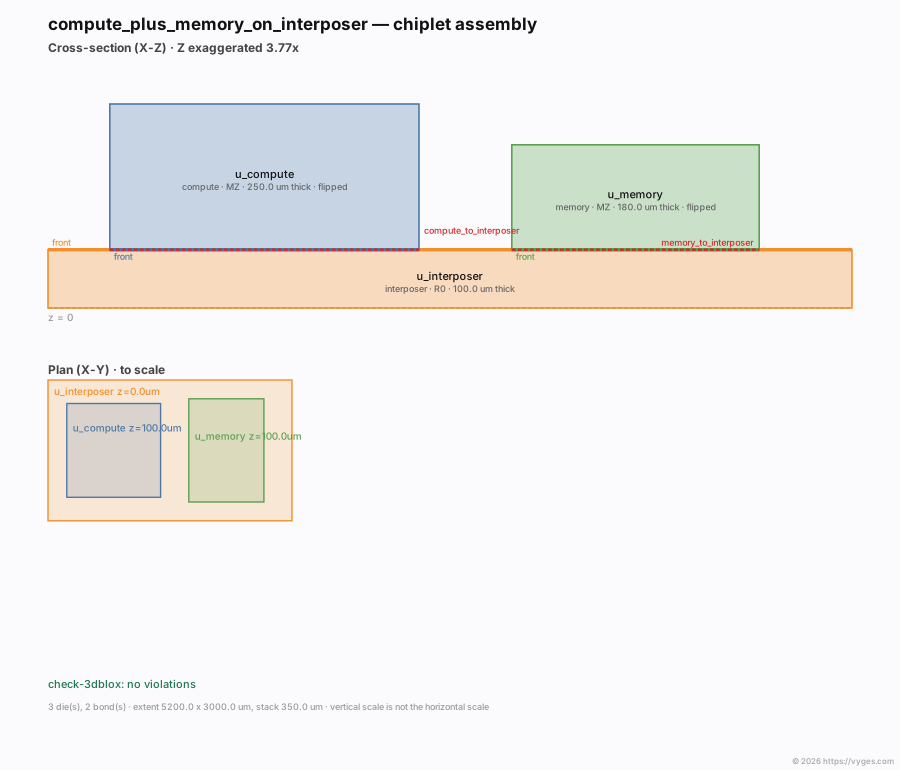
A 2.5D assembly: two dies side by side on an interposer, seen in cross-section above and from above below. Self-contained SVG or PNG, so it commits to a repository and uploads as a CI artifact. The first post explains how to read one.
What is not solved
Being precise here matters, because "chiplet support" is being used loosely.
You cannot yet time a 3D stack with these tools — cross-die parasitic extraction and timing need database classes that do not exist upstream yet. A truly heterogeneous stack, where each die sits on a different process, cannot be fully represented either, because a design database holds one technology. That one is awkward, given that heterogeneity is the entire premise of chiplets.
And there is a bigger absence. For monolithic ASICs, OpenROAD supplies the engines and OpenLane 2 / LibreLane supplies the flow. Open-source chiplet assembly has no equivalent orchestration layer yet — that is where this goes next, and the third post makes the case for why the model and the checks had to come first.
Those are real gaps and we would rather name them than let the phrase imply they are done. They are also the roadmap.
What is solved
An engineer with two dies and an assembly description can now find out whether their chiplet interface is real — before it is silicon, on their own machine, with tools they can read the source of.
That matters most to the people who were furthest from this: research groups exploring heterogeneous integration, university programmes teaching packaging without a tool budget, small teams building a multi-die product for the first time, and anyone who wants to understand what their assembly description actually means rather than trusting a black box to tell them.
It is narrower than "chiplet support". It is also a beginning, and it is open.
curl --proto '=https' --tlsv1.2 -LsSf \
  https://github.com/vyges-tools/cli/releases/latest/download/vyges-installer.sh | sh
export PATH="$HOME/.vyges/bin:$PATH"
vyges install loom
The technical detail
Three companion posts cover the whole thing properly:
- Describing and Checking a Chiplet Stack, With Open Tools — the assembly model: how a stack is described in 3Dblox, read into OpenDB, validated and visualized.
- Your Chiplet Interface Passes Every Open-Source Check. It's Still Dead. — why structural verification is not electrical verification, and what
check-d2ddoes about it. - An Open Chiplet Flow, End to End, on OpenROAD — the complete workflow, from a 3Dblox file to a CI gate, with a five-minute demo.
Built on OpenROAD's OpenDB (BSD-3-Clause). vyges-opendb ships in the Vyges Loom open EDA suite (Apache-2.0). Corrections, counter-examples and questions are welcome — particularly from anyone who has done this in a packaging house and can tell us what we have missed.